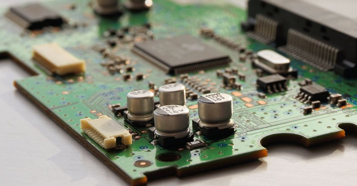
Unifying the Hardware Development Pipeline
A recent analysis published by TechPowerUp outlines a streamlined approach to printed circuit board (PCB) prototyping that bridges the gap between design and physical production. The report details how EasyEDA, a web-based electronics design automation tool, integrates directly with JLCPCB’s manufacturing services. This connection allows engineers to move from schematic capture and layout directly to fabrication without manual file conversions or disjointed vendor interactions.
The workflow encompasses critical steps such as design rule checking, component sourcing, and final assembly specifications. By linking these stages, the process aims to eliminate the traditional silos that often exist between hardware designers and manufacturing partners. This integration is particularly relevant for hobbyists and small engineering teams who previously had to manage multiple separate platforms to get a functional prototype built.
Reducing Friction in Complex Board Designs
The significance of this integrated workflow lies in the increasing complexity of modern electronic products. As devices demand smaller footprints and higher density, the margin for error in PCB layout shrinks significantly. High-speed interfaces, multilayer structures, and fine-pitch components leave little room for manufacturing mistakes. Traditionally, each handoff between design, sourcing, and assembly created opportunities for data to become outdated or misaligned. For instance, a component might become unavailable after the layout is complete, or a fabrication constraint might necessitate a routing change that was not accounted for in the initial design.
By moving these checks earlier in the development cycle, the unified platform helps identify potential issues before they reach the factory floor. This proactive approach reduces the risk of costly re-spins and delays, which are common pain points in hardware development. It also simplifies the technical burden on users who may not have deep expertise in manufacturing constraints, allowing them to focus more on functionality and less on logistical coordination.

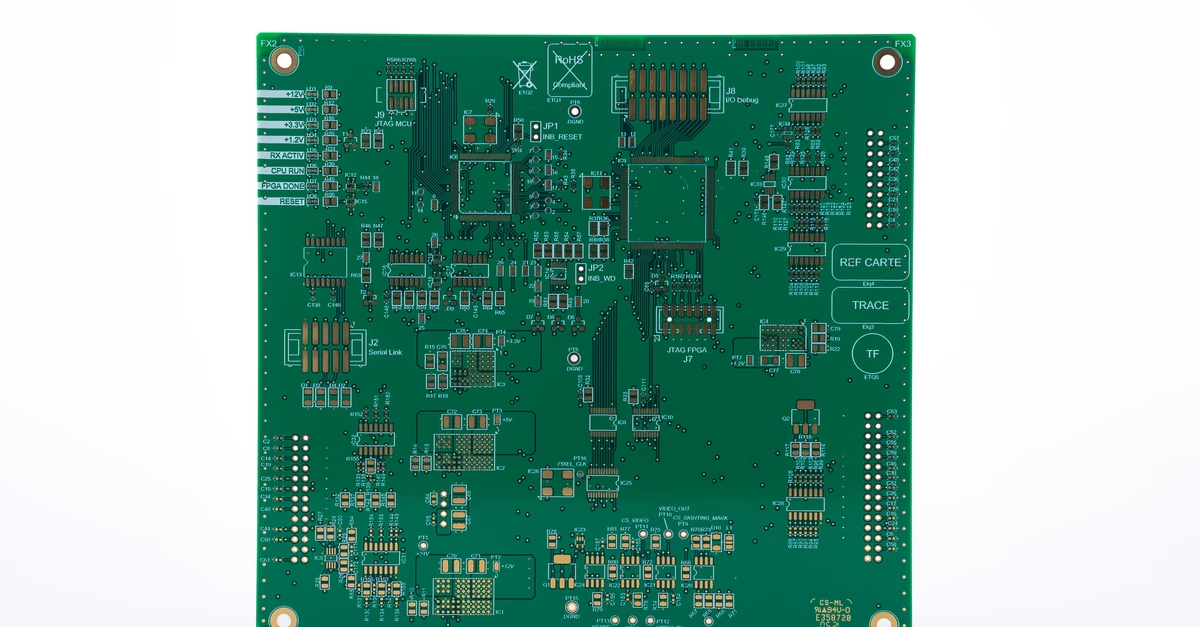
Implications for Canadian Makers and Engineers
For Canadian makers and independent engineers, this shift toward integrated prototyping tools represents a practical reduction in barriers to entry. While the specific pricing and turnaround times for JLCPCB services can vary based on order volume and complexity, the structural benefit of a connected workflow remains consistent. Users can expect a smoother transition from digital design to physical product, provided they adhere to the design guidelines supported by the platform.
However, it is important to note that while the software facilitates the process, it does not eliminate the need for careful design planning. Engineers must still ensure their schematics are robust and their component selections are viable. The primary value proposition here is efficiency: fewer manual steps mean fewer chances for human error. As hardware development continues to evolve, tools that prioritize seamless integration will likely become the standard for rapid prototyping, offering a clearer path from concept to finished PCBA for those working outside large corporate R&D departments.